- Home
- SCDM 2025
Invited Speakers
Invited Speakers
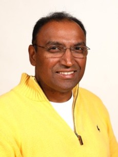
Prof. Sridhar Govindarajan
Professor, De Montfort University, UK
Title:Current Perspectives in Smart Energy Storage Technologies: Advances and Challenges in Battery Systems
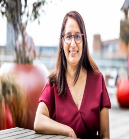
Prof. Shushma Patel
Pro Vice Chancellor Artificial Intelligence, Dean Faculty of Technology, Arts and Culture, Professor of Information Systems. De Montfort University, UK
Title:AI, Sustainability and future of Higher Education
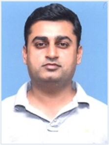
Mr. Yogesh Verma
Head,Cyber Security and Networks Division,Space Applications Centre, ISRO, Ahmedabad
Title:Cyber Security - Threat Landscape, Security controls & Research Opportunities

Dr. Anuradha Kar
Aivancity, La Grande École de l’Intelligence Artificielle et de la Data Paris, France
Title:Agentic AI for Smart Engineering: Opportunities and Challenges for a Sustainable Future
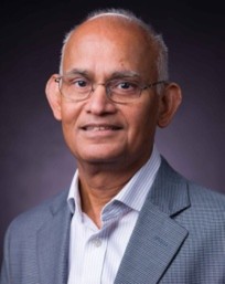
Mr. Arun K. Somani
Distinguished Professor and Senior Associate Dean,Electrical and Computer Engineering,College of Engineering, Iowa State University, USA
Title:Using Fault Tolerance in AI: Reliable and Robust Early Skin Cancer Detection
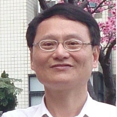
Name: Kuei-Shu Chang-Liao
Designation: Professor
Department: Department of Engineering and System Science, National Tsing Hua University, TAIWAN
Email: lkschang@ess.nthu.edu.tw
About Speaker:
Kuei-Shu Chang-Liao received the B.S. and M.S. degrees in Telecommunication and Electronics from National Chiao Tung University in 1984 and 1989, respectively, and the Ph.D. degree in Electrical Engineering from National Taiwan University in 1992. In 1992, Dr. Chang-Liao joined the faculty at the National Tsing Hua University where he has been a Professor of Department of Engineering and System Science since 1999. In 2000, he was a visiting research fellow at the Department of Electrical Engineering of Yale University, where he was involved in Flash memory and charge pumping measurement. During 2007-2010, he served as the Associate Chairman of Department of Engineering and System Science, and served as the Chairman during 2022-2024. His current research interests include high-k/metal gate stack processes in FinFET/GAAFET, Ge or SiGe MOS devices, charge-trapping flash memory devices, trap analysis in MOS device by charge pumping measurement, and radiation effects on semiconductor devices. Dr. Chang-Liao is a Distinguished Lecturer of IEEE EDS, senior member of IEEE, and member of the Electrochemical Society. He served as the Editor of IEEE Electron Device Letters during 2012-15. He received the excellent Industry-Academic Research Award from Ministry of Education in 2003. He has published over 400 papers in prestigious journals and conferences. He has chaired and served as committee members in several international conferences.
Title: High Performance High-k Gated SiGe/Ge CMOS Devices with Low Temperature Process
Abstract:
Process development of gate stack and channel in CMOS device is the key challenge beyond sub-3 nm technology node. The application of high-k dielectric or alloy in gate stack demonstrates both low EOT and gate leakage current. However, carrier mobility degradation caused by high-k gate dielectric is an issue for high performance device. SiGe/Ge channel is promising to replace Si due to its higher carrier mobility and compatible material properties. Since the properties of high-k/Ge interfaces are usually poor, the interface quality is a critical issue to realize high performance Ge MOSFETs. In this talk, engineering interface and buffer layers for SiGe/Ge MOSFETs, Ge n/p-FinFETs with super-critical fluid treatments, and n/p-FinFETs with SiGe/Si super-lattice channel will be presented. Low EOT, low gate leakage current, and high mobility in SiGe/Ge FinFET/GAAFET can be simultaneously achieved.
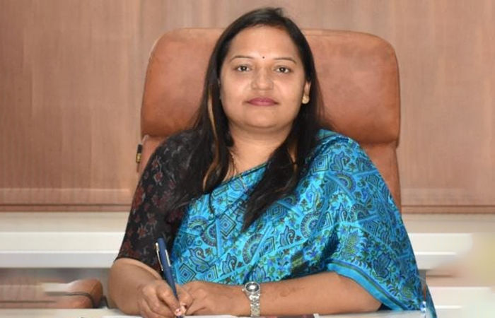
Name: Ms. Neha Kumari, IAS
Designation: Mission Director
Department: Gujarat State Electronics Mission (GSEM) Government of Gujarat
About Speaker:
Ms. Neha Kumari, IAS, a young and dynamic officer from the 2015 batch of Indian Administrative Services (IAS). She has taken charge as the Mission Director of the Gujarat State Electronics Mission (GSEM) on April 15th, 2025. GSEM serves as the nodal agency spearheading Gujarat's vision to establish itself as a global hub for Electronics and Semiconductor Manufacturing.
Ms. Neha Kumari holds a degree in Electrical and Electronics Engineering from the Birla Institute of Technology, Mesra, and a master’s degree in public management from Jawaharlal Nehru University (JNU). She has previously held several significant administrative positions, including District Collector, Deputy Municipal Commissioner at the Ahmedabad Municipal Corporation, and District Development Officer (DDO) among others.
With a distinguished career characterized by administrative excellence and visionary leadership, Ms. Neha Kumari brings extensive experience in governance, policy implementation, and industry collaboration. Her appointment comes at a crucial time as Gujarat intensifies its investments in the Electronics System Design and Manufacturing (ESDM) sector, leveraging its robust policy framework, infrastructure ecosystem, and investor-friendly climate.
Name: Hens-Tung (Becker)
Designation: PhD Professor
Department: International College of Semiconductor Technology National Yang Ming Chiao Tung University, Taiwan
Title: Design Techniques for the Boost of Operating Frequency
Abstract:
The advancement of the next-generation wireless communication system has imposed very stringent requirement on the implementation of the RF front-ends. In order to maintain the demanded quality-of-service featuring ultra-high data transmission rate and ultra-low latency, a very wide and contiguous operation bandwidth is a must. Since the frequency bands below S-band have been congested with commercial applications, migration of the operating frequencies into millimeter-wave range is necessary. This fact could be evidenced by the frequency allocation of the 5G/B5G communications systems.
Practically, the unavoidable higher loss, including the propagation loss and the metallic/dielectric loss, at high frequencies makes the circuit design very challenging. Other than the loss issues, the fast gain degradation of the device with respect to operating frequency is natural and limits the performance of the power amplifiers. Thus, how to overcome such challenges using circuit approach is an interesting research topic. In this talk, we will discuss two possible solutions, namely, the dominant pole push away and loss minimization techniques. Both the theoretical fundamentals and the experimental verifications will be presented.
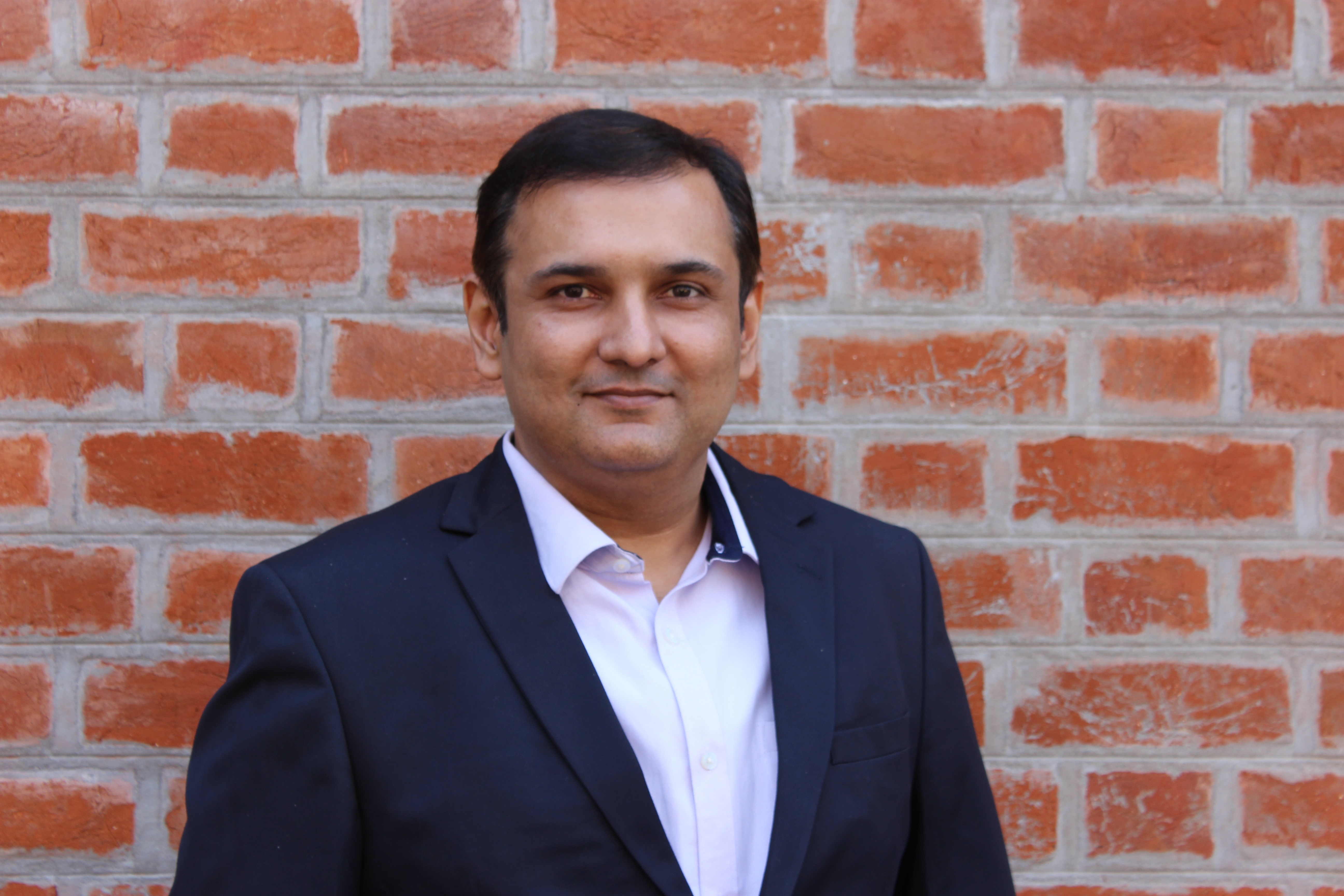
Name: Mr. Maunang Gor
Designation: Vice President, Integrated Circuits Design | Sasken Silicont
About Speaker:
Maunang is currently working as Vice President, IC Design and India delivery head. Maunang has 19 years of distinguished experience in the semiconductor industry, with deep specialization in high-speed IO and PHY design across advanced process nodes, spanning from 65nm to the cutting-edge 2nm technologies. His career reflects a strong blend of technical depth and strategic leadership, having held pivotal roles at industry-leading organizations such as Synopsys, Intel, AMD, and Open-Silicon. Complementing this experience is an outstanding academic foundation, a Post Graduate Diploma in Advanced Business Analytics from IIM Ahmedabad and a Master’s in Microelectronics from BITS Pilani, equipping Maunang with the perfect blend of technical depth and strategic insight. He has successfully led and delivered complex IP development programs, consistently driving innovation and excellence in execution. A seasoned collaborator, Maunang has effectively engaged with cross-functional and cross-cultural teams across North America, Israel, Taiwan, and beyond, bringing a truly global perspective to design and development processes.
Name: Dr. Dipesh Panchal
Company: eInfochips, Ahmedabad, India
Title: Quantum world Insights of evolution, application and challenges.
Abstract:
To solve complicated computational problems that are unsolvable for conventional systems, the increasing interdisciplinary topic of quantum artificial intelligence, or quantum AI, blends the ideas of artificial intelligence and quantum computing. Recent developments in hybrid quantum-classical frameworks and quantum hardware have made it possible to investigate quantum-enhanced models for tasks such as decision- making, pattern recognition, and natural language processing. Quantum AI has the potential to transform a wide range of industries, from cybersecurity and autonomous systems to drug research and financial modeling. This presentation emphasizes the core ideas, recent developments, and possible applications of quantum artificial intelligence (AI), along with QCA terminology.
Name: Dr. Jignesh Patoliya
Company: eInfochips, Ahmedabad, India
Title: Quantum world Insights of evolution, application and challenges.
Abstract:
To solve complicated computational problems that are unsolvable for conventional systems, the increasing interdisciplinary topic of quantum artificial intelligence, or quantum AI, blends the ideas of artificial intelligence and quantum computing. Recent developments in hybrid quantum-classical frameworks and quantum hardware have made it possible to investigate quantum-enhanced models for tasks such as decision- making, pattern recognition, and natural language processing. Quantum AI has the potential to transform a wide range of industries, from cybersecurity and autonomous systems to drug research and financial modeling. This presentation emphasizes the core ideas, recent developments, and possible applications of quantum artificial intelligence (AI), along with QCA terminology.
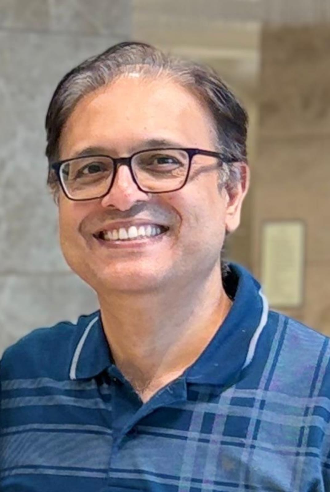
Name: Mr. Jwalant Joshipura
Designation: Senior Director, NXP Semiconductors, Bangalore, India
About Speaker:
Jwalant Joshipura is Senior Director at NXP Semiconductors, leading IC design for the ADAS and Automotive Radio business lines. With 25+ years of experience in VLSI and SoC design, he has held key technical and leadership roles at STMicroelectronics and now at NXP, driving complex chip development from architecture to mass production. He is also active in academia, having served as guest faculty at Galgotias University and Reva University. Jwalant holds one U.S. patent, multiple publications, and holds degrees from BVM, VV nagar and BITS Pilani.
Title: Advances in Semiconductor ICs and Systems: Transforming Automotives to Robots on Wheels
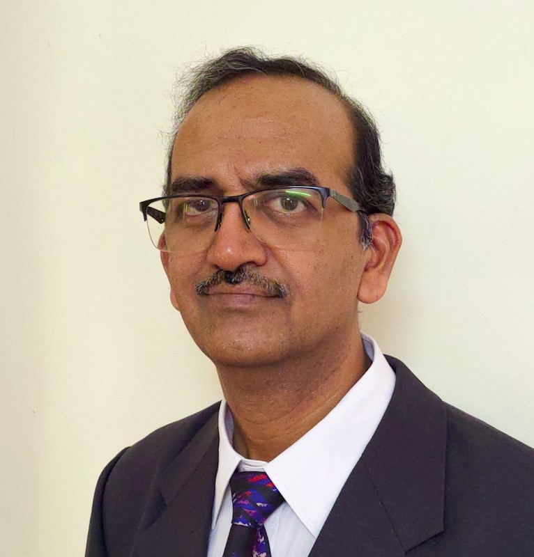
Name: prof.Ajay agarwal
Designation: Professor
Department: Department of Electrical Engineering, Indian Institute of Technology, Jodhpur
About Speaker:
Ajay Agarwal is Professor, EE Dept, IIT Jodhpur; adjunct faculty at Centre of MedTech, and Centre for AIOT and Application; CEO, AIOT Innovation Hub Foundation; etc. at IIT Jodhpur. Prof. Ajay is Director, Electronics Sector Skills Council of India (ESSCI) and Sahasra Semiconductors. He is also founding Director of a startup - Sarbit Innovations and mentor of another startup - Caldor Health Technologies.
Earlier, he worked at CSIR-CEERI, Pilani as Sr Principal Scientist & Coordinator-Smart Sensors Area; Associate Dean, Engineering Sciences at AcSIR, New Delhi.
He also served at Institute of Microelectronics, Singapore as Member of Technical Staff, Adjunct faculty National University of Singapore & Nanyang Technological University, Singapore, and Semiconductor Complex Ltd., Chandigarh & USHA India, Faridabad.
Ajay is involved in the development of Nanotechnologies, MEMS, micro fluidics and Micro-sensors for Environmental monitoring, Healthcare and Industry 4.0 applications. He has ~310 research publications, >110 invited/ plenary/ keynote talks and 40 patents (granted or filled). He has supervised 19 Ph.D. students and is guiding 14 PhD students.
He is Sr. member, IEEE, USA since 2006 and Vice-Chairperson, IEEE Rajasthan Subsection (2021, 2023 & 2024); Life Fellow, IETE (India), Semiconductor Society of India, MSI (India), & The Institution of Engineers (India), & member IAAM-International Association of Advanced Materials, Sweden & MRS, Singapore [till 2009] etc.
Prof. Agarwal is bestowed with various awards including:
- Chief Editorial Advisor (Microelectronics and Semiconductors) at BytesWall, a tech-media platform since 2025.
- Research Excellence-2024, Senior Researcher Award (Engineering), IIT Jodhpur.
- 2021 - IETE Bapu Seetha Ram Award.
- Outstanding Engineering Services to Society Award 2021, The Institute of Engineers (India), Rajasthan State Centre, Jaipur.
- 2020 - CSIR Technology Award (Innovation).
- 2013 - DST-UKIERI Thematic Partnerships Award, India.
- 2008 - National Technology Award, Singapore.
- 2009 - Excellence Award, IME Singapore.
- Collaboration Development Award, British High Commission, Singapore - 2005 & 2006.
- Super Kaizen (4 times) and Best Kaizen (7 times) at USHA (India) Ltd.
His biography is included in the Who's Who in the World, which profiles the most accomplished men and women in the world since 2010 & in Who's Who in Asia since 2012.
Web page: ajayagarwal.co.in
Group webpage: https://sites.google.com/iitj.ac.in/rims/home?authuser=0
Title: Opportunities in the Emerging Indian SEMICON Ecosystem
Name: Dr.Philippe Maurin
Designation: Scientific and Higher Education Attaché at the French Embassy in India.
About Speaker:
Dr Philippe Maurin is Scientific and Higher Education Attaché at the French Embassy in India. He is based at the French General Consulate in Mumbai, his missions are to develop academic cooperation between France and Western India States (Gujarat, Maharashtra, Madhya Pradesh, Chhattisgarh and Goa), promoting French attractivity for studies, institutional partnerships, research and innovation cooperation, as well as building bridges between public and private research.
His primary job is Associate Professor in Organic Chemistry at the Ecole Normale Supérieure (ENS) in Lyon, a leading research-intensive institution in France
Before his current position, he was the Director of International Affairs at Ecole Normale Supérieure de Lyon from 2018 to 2023.
From 2015 to 2018, he was stationed at the French Consulate General in Wuhan as Attaché for Science and Technology.
Before 2015 he has been advisor of the Vice-president of studies of ENS de Lyon for careers and studies in exact and experimental sciences and has been the Director of the chemistry department of ENS de Lyon from 2010 to 2014.

Name: Ms. Chandni Patel
Designation: Sr. Physical Desgin Engineer (Level 2) at eInfochips an Arrow Company
About Speaker:
Session on Placement and Routing – Dive into Backend VLSI from floorplan to routing with advanced lower technology nodes. Physical backend design flow involves translating a synthesized netlist into a manufacturable layout. It includes floor planning, placement, clock tree synthesis, routing, and physical verification. Timing, power, and area constraints are optimized throughout the process. The final output is a GDSII file ready for fabrication.
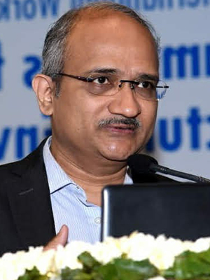
Name: Prof. V Ramgopal Rao
Designation: Group Vice-Chancellor, Birla Institute of Technology & Science, Pilani & Former Director, IIT Delhi, India
About Speaker:
Prof. V. Ramgopal Rao is currently the Vice-Chancellor for the Birla Institute of Technology & Science (BITS) Pilani group of institutions. Prior to joining the BITS Group in 2023, Prof. Rao had served as the Director of IIT Delhi for 6 years during 2016-2021 and as a Chair Professor for Nanoelectronics at both IIT Bombay and IIT Delhi.
Prof. Rao is a Nanoelectronics researcher with over 500 research papers and 50 patents, which include 20 issued US patents. 15 of his patents have been licensed to industries for commercialization. The IP on CMOS-SoC applications developed in his group is now used in 100's of millions of ICs sold all over the world. Prof. Rao is a co-founder of two deep technology startups at IIT Bombay ( Nanosniff & Soilsens ) which have successful commercial products in the market. For his research accomplishments, Dr. Rao has been elected a Fellow of IEEE, a Fellow of The World Academy of Sciences (TWAS), the Indian National Academy of Engineering (INAE), the Indian Academy of Sciences (IASc), the National Academy of Sciences (NASI) & the Indian National Science Academy (INSA). 52 Ph.D. students have graduated so far under his supervision and are working in leading academic institutions, semiconductor industries all over the world, including in India.
Prof. Rao's research and leadership contributions have been recognized with over 35 awards and honors in the country and abroad. He is a recipient of three honorary doctorates. The recognitions Prof. Rao received include the Shanti Swarup Bhatnagar Prize in Engineering Sciences, Infosys Prize, IEEE EDS Education Award and many others. Prof. Rao serves on the Editorial Advisory Boards of several leading international journals such as the ACS Nano Letters, AIP Applied Physics Reviews, IEEE Journal on Flexible Electronics etc. Dr. Rao has delivered over 200 Plenary, key-note and invited lectures all over the world.
Prof. Rao is an internationally acclaimed Nanoelectronics researcher with over 500 research papers and over 50 patents, which include 20 issued US patents. 15 of his patents have been licensed to industries for commercialization. The IP on CMOS-SoC applications developed in his group is now used in 100's of millions of ICs sold all over the world. Prof. Rao is a co-founder of two deep technology startups at IIT Bombay ( Nanosniff & Soilsens ) which have successful commercial products in the market. Besides his education and research activities, Prof. Rao is also well known for establishing major Nanoelectronics Programmes in India. For his research accomplishments, Dr. Rao has been elected a Fellow of IEEE, a Fellow of The World Academy of Sciences (TWAS), the Indian National Academy of Engineering (INAE), the Indian Academy of Sciences (IASc), the National Academy of Sciences (NASI) & the Indian National Science Academy (INSA). 52 Ph.D. students have graduated so far under his supervision and are working in leading academic institutions, semiconductor industries all over the world, including in India.
Prof. Rao's research and leadership contributions have been recognized with over 35 awards and honors in the country and abroad. He is a recipient of three honorary doctorates. The recognitions Prof. Rao received include the Shanti Swarup Bhatnagar Prize in Engineering Sciences, Infosys Prize, IEEE EDS Education Award (the highest international award bestowed by IEEE Electron Devices Society for Education) and many others. Prof. Rao serves on the Editorial Advisory Boards of several leading international journals such as the ACS Nano Letters, AIP Applied Physics Reviews, IEEE Journal on Flexible Electronics etc. Dr. Rao has delivered over 200 Plenary, key-note and invited lectures all over the world.
Besides his regular responsibilities at BITS Pilani, Prof. Ramgopal Rao serves as a Chairman for multiple committees at the National level related to Education, Research and Innovation programmes in India. He is currently the Chairperson, Council of Management (BoG) for the Jawaharlal Nehru Centre for Advanced Scientific Research (JNCASR) in Bangalore and Chairperson, Board of Governors for the National Institute of Food Technology Entrepreneurship and Management (NIFTEM) in Haryana, two premier institutions of Govt of India.
Title: Advancing IoT Sensor Networks in the Developing World: The Role of MEMS/NEMS Platforms in Overcoming Key Challenges
Abstract:
IoT based sensor networks are expected to see a massive growth the world over in the next few years. However, the poor infrastructural facilities available in many of the developing countries and meeting of the low-cost requirements in these markets can pose two major challenges for a massive deployment of IoT sensors in the developing world. Sensor networks for security, healthcare, environment and agriculture are some of the areas where IoT can significantly impact the world populations.
While silicon has been the most widely used material for Nanoelectronics and Micro/Nano-Electro-Mechanical-Sensor systems, polymers enable fabrication of MEMS/NEMS devices with superior electro-mechanical characteristics as compared to the traditional silicon-based materials. Polymers are also ideally suited for low cost disposable sensor applications, as well as for applications that require high surface stress sensitivity. The applications for polymer MEMS/NEMS range from healthcare to homeland security. There are however multiple issues that need to be addressed in order to make the polymer MEMS a mainstream technology. One of the issues is related to the electro-mechanical transduction sensitivity, which requires integration of novel materials and process techniques. The other issue concerns the stability of polymer materials in atmosphere, when used as sensors. CMOS compatibility of these materials processing is another issue. In this talk, we will look at some of the approaches for addressing these concerns using a variety of processes & materials. This talk discusses the current status of research with polymer MEMS/NEMS devices and use of organics for enhancing the performance of silicon devices.
